How is a Zener diode fabricated? What causes the setting up of high electric field even for small reverse bias voltage across the diode? Describe, with the help of a circuit diagram, the working of Zener diode as a voltage regulator.
OR
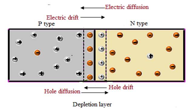
(a) Explain with the help of a diagram, how depletion region and potential barrier are formed in a junction diode.
(b) If a small voltage is applied to a p-n junction diode how will the barrier potential be affected when it is
(i) forward biased, and
(ii) reverse biased?
Zener diode is a heavily doped diode from both p and n sides of the junction. Due to heavy doping, a very thin (<10−6 m) depletion region is formed between the p and n sides, which results into the electric field of the junction to be extremely high (~5 × 10⁶ V/m) even when a small reverse voltage of about 5V is applied.
Zener diode as a voltage regulator:
To get a constant d.c. voltage from the d.c. unregulated output of a rectifier, a Zener diode can be used. The circuit diagram of a voltage regulator using a Zener diode is shown in the figure below.
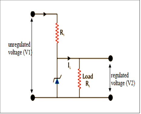
The unregulated d.c. voltage is connected to Zener diode through a series resistance Rs in such a way that the Zener diode is reverse biased. When the input voltage increases, the current through Rs increases and hence through the Zener diode also increases. Due to this, the voltage drop across Rs also increases but there is no change in the voltage across the Zener diode. This is because the Zener voltage remains constant in the breakdown region even though the current through it changes. Similarly, when the input voltage decreases, the current through Rs and the Zener diode also decreases. The voltage across Rs decreases without any change in the voltage across the Zener diode. Thus, any increase or decrease in the input voltage results in an increase or decrease of the voltage drop across Rs without any change in the voltage across the Zener diode. Hence, the Zener diode acts as a voltage regulator.
OR
The diode is a device which is made up of p-type semiconductor and n-type semiconductor fussed to form junction, as shown in the figure. P-type semiconductor has holes as charge carriers and n-type semiconductors has electrons as charge carriers. The electrons on n-type when meet holes from p-type they diffuse and form a region called depletion layer at the junction. The electrons from n-type accumulated towards p-type while holes from p-type accumulated towards n-type. This accumulation of charge carriers in junction repels the further diffusion of electrons and holes and a barrier is formed between electrons and holes. This barrier is called potential barrier.
(b) (ii) When p n junction diode is forward biased, that means p-type is connected to positive terminal of the battery and n-type is connected to the negative terminal of the battery. Then the holes from p-type will be repelled by the positive terminal of the battery and they will move towards the junction. Similarly, electrons will be repelled by the negative terminal of the battery and they will also move towards the junction of the diode. This will in return reduce the thickness of the depletion layer and the potential barrier will also decrease.
On the other hand, when the diode is reversed biased, it means that the p-type will be connected to the negative terminal and n-type will be connected to the positive terminal of the battery. The electrons from n-type will move towards the battery terminal and similarly holes will also move towards the battery terminal (positive). Hence the depletion layer will increase in width and potential barrier will also increase.