With the help of a circuit diagram, explain the working of a junction diode as a full wave rectifier. Draw its input and output waveforms. Which characteristic property makes the junction diode suitable for rectification?
Consider the following circuit diagram of a full wave rectifier.
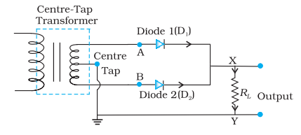
Let the input voltage in the first half cycle of AC signal be such that the voltage at A is positive and voltage at terminal B is negative. So, diode D1 gets forward biased and conducts (while D2 being reverse biased won’t conduct). Hence, during this half cycle we get an output current (and a output voltage across the load resistor RL). In the course of the AC cycle when the voltage at A becomes negative with respect to centre tap, the voltage at B would be positive. In this part of the cycle diode D1 would not conduct but diode D2 would, giving an output current and output voltage (across RL) during the negative half cycle of the input ac. Thus, we get output voltage during both the positive as well as the negative half of the cycle, i.e. the full input wave signal gets rectified.
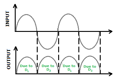
From the V-I characteristic of a junction diode we see that it allows current to pass only when it is forward biased. So if an alternating voltage is applied across a diode the current flows only in that part of the cycle when the diode is forward biased. This property is used to rectify alternating voltages and the circuit used for this purpose is called a rectifier.