When is a transistor said to be in active state? Draw a circuit diagram of a p-n-p transistor and explain how it works as a transistor amplifier. Write clearly, why in the case of a transistor (i) the base is thin and lightly doped and (ii) the emitter is heavily doped.
If the emitter- base junction is forwards biased and base collector junction is reverse biased, such that the forward current is sufficient to send, then the transistor is called in active state.
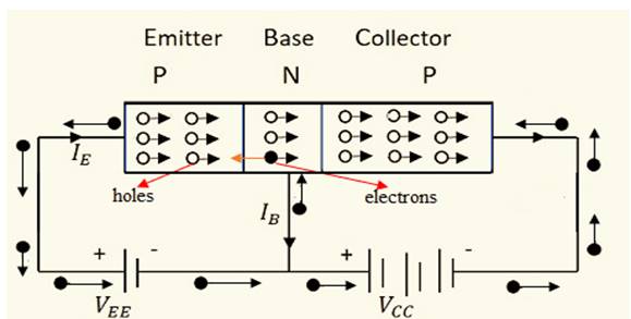
The circuit diagram of a p–n–p transistor is as shown below:
A transistor when operated in the active state then it acts as an amplifier. The working principle of a common emitter transistor as an amplifier is that a weak input signal given to the base region which produces an amplified signal as output in the collector region. The circuit diagram for a p–n–p common emitter transistor amplifier can be shown in the figure:

The emitter base junction is forward biased by the battery VBB and the battery VCC reverse biases the emitter collector region. The e.m.f. of the voltage supplies should be greater than the barrier potential across the junctions of base-emitter and collector emitter. The output current produces a potential difference across the load resistance RL. A weak alternating signal is applied between the base and the emitter. When the signal increases in the positive direction, the base current also increases. The base current is amplified βtimes and appears at the collector. The collector current flowing through the collector load resistance produces a voltage. This output voltage is equal to the collector current times the load resistance. Thus, an amplified output is obtained. The voltage gain = output voltage/input voltage.
In a transistor, the base is thin and lightly doped so that it contains smaller number of majority carriers. This reduces the recombination rate of free electrons and holes in the base region when the majority carriers go from the emitter to the collector. On the other hand, the emitter region in a transistor is heavily doped because the emitter supplies the majority carriers for the current flow.
Couldn't generate an explanation.
Generated by AI. May contain inaccuracies — always verify with your textbook.